Example: FinFET
The FinFET exploits the third dimension in order to achieve better control of the current flow in the channel. From the simulation point of view, this requires a shift from established two-dimensional device simulations to fully three-dimensional ones. Thanks to the abstract approach to grid handling in ViennaGrid, ViennaSHE is able to simulate three-dimensional devices already in the very first release.
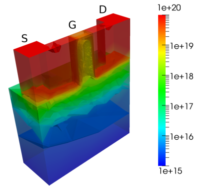
As an example, we consider a FinFET with applied gate voltage of 0.8 Volts and a drain-source bias of 0.3 Volts. Doping profiles are again chosen constant in each segment of the device for simplicity.
Since the device is symmetric with respect to the fin, the FinFET is slit along this plane of symmetry and only half of the device is simulated. The electron concentration ( ) shown below shows the accumulation of electrons near the gate oxide.
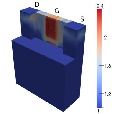
Unfortunately, the four-dimensional simulation space (three spatial coordinates plus one energy coordinate) cannot be plotted reasonably, for which reason we have to refrain from a plotting the distribution function. Nevertheless, adaptive expansion orders can still be employed. The average expansion order with respect to energy at each point in the device is plotted below. Note that the channel regions are well resolved.